17607506214
All other trademarks are the property of their respective owners
The CDCLVD1208 clock buffer distributes one of two selectable clock inputs (IN0 and IN1) to 8 pairs of differential LVDS clock outputs (OUT0 through OUT7) with minimum skew for clock distribution. The CDCLVD1208 can accept two clock sources into an input multiplexer. The inputs can either be LVDS, LVPECL, or LVCMOS.
The CDCLVD1208 is specifically designed for driving 50-Ω transmission lines. In case of driving the inputs in single-ended mode, the appropriate bias voltage, VAC_REF, must be applied to the unused negative input pin.
The IN_SEL pin selects the input which is routed to the outputs. If this pin is left open, it disables the outputs (static). The part supports a fail-safe function. The device incorporates an input hysteresis which prevents random oscillation of the outputs in the absence of an input signal.
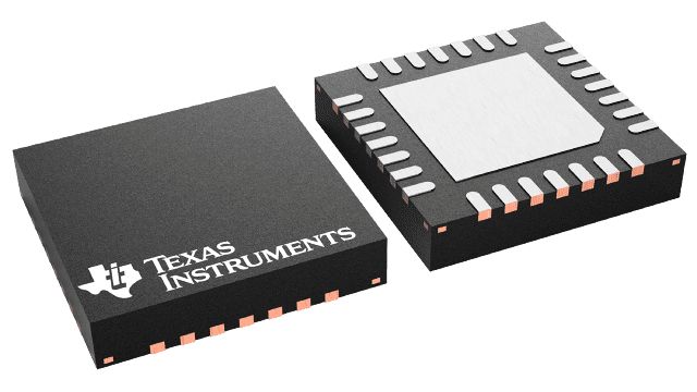
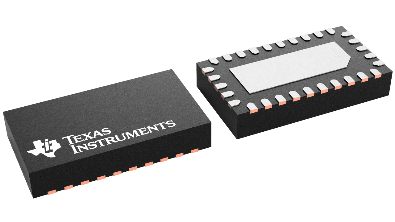
The device operates in 2.5-V supply environment and is characterized from –40°C to 85°C (ambient temperature). The CDCLVD1208 is packaged in small, 28-pin, 5-mm × 5-mm VQFN package.
從線上下單到出貨與金流,我們以穩定交期與安全流程,協助您放心備料。
採少量多樣計價與快速報價機制,搭配自有電子料倉, 支援急單需求,最快 24 小時即可交貨。
庫存料號下單後優先處理,可搭配分批出貨與 不同收貨地點,縮短開發與備料時間。
支援多家第三方支付與信用卡,全程加密處理交易, 不保留卡號資訊,金流與資料安全有保障。
.png)